Zero Sized Intelligence,Quantum Control: New Evolution in Technology
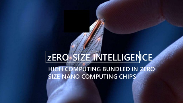
Zero Size Technology
Quantum control uses a technology derived from physics for computer application QED, describes the interaction of matter and light, and
QED circuits take this interaction to the computer chip by trying to harness the interaction for circuitry in machines. Let’s go through what quantum control 1st all about. Its location is in center of an emerging technology known as circuit-QED, in which photons trapped on a silicon chip are made to interact with superconducting devices called artificial atoms, which have various energy levels just like real atoms. Circuit-QED items alters quantum information as it is transmitted from light to matter and vice versa. But before we can do that we need a way to manipulate the quantum information that photons carry.
And nobody has worked out a good way to do that. Today, however, University of Maryland says they know how to do it. Their idea Is the phonic equivalent of circuit QED. So instead of trapping a photon in a cavity and make it interact with an artificial atom, they want to do it with phonon: quantum phonographic . Similar to Photons, Phonon are sound- activated quantum vibrations that move Circuitry and motor machines at the chip level. Phonon are quantum vibrations that travel through the lattice that makes up materials, much n the same way that
Sound passes through the air. Since any quantum object can also carny quantum information, various physicists are thinking about ways of using phonon for quantum computation. The scheme is relatively straight forward. It begins by creating a silicon membrane-a One dimensional silicon crystal about 200 nano meters thick. The engineering the properties of this membrane, a kind of wave guide that steers phonon is created. A laser is used to create a phonon by zapping this membrane, which sends a quantum packet of vibration through the lattice.

This atom trapped in an optical cavity distorts the lattice. It Is this distortion that interacts with the photon. However, an external magnetic field can be used to make the distortion and take i lake several different energy levels. These changes the way the phonon interacts in a way hat processes the information l carries. Finally, the phonon passes into another region of the silicon lattice with a band gap that has been engineered to convert the phonon into a photon, which can their be measured and calibrated to Our desired impulse or information. That sounds like a good plan. So the Only question is over the feasibility of the design for quantum phonon dynamics. T he difficulty, of course, will be building this thing, Which as the University say will be seminal achievement. This is a beautiful demonstration of controlling matter at the atomic Scale to make a real device, isn’t it?
Fifty years ago when the first transistor was developed, 10 one could have predicted the role that Computers Would play in our society today. As we transition to atomic-scale devices, We are now entering a new paradigm where quantum mechanics promises a similar techno Logical disruption. Researchers are Working to build a single-atom transistor as a first step to the development of a quantum computer that works by Controlling the electrons and quantum information, or quits. The atom sits in a well or channel, and for it to operate as a transistor the electrons must stay in that channel, which seems to be a major challenge as at higher temperatures, the electrons move more and go outside of the channel. For this atom to act like a metal you have to contain the electrons to the channel. II someone develops a technique to contain the electrons, this technique could be used to build a computer that would work at room temperature.
But this is a fundamental challenge for this technology. Although definitions can vary, simply stated Moore’s Law holds that the number of transistors that can be placed on a processor will double approximately every 18 months. The latest Intel chip, the ‘Sandy Bridge, uses a manufacturing process to place 2.3 billion transistors 32 phosphorus atom, by comparison, is Just 0.1 nano meters across, which would significantly reduce the size of processors made using this technique, although it may be many years before single-atom processors actually are manufactured. But once technology gets there a critical nano meters apart.A single question might be “Is Single-Atom Transistor an End of Moore’s Law and May Be Beginning of Quantum Computing?” Futurist sees the future advance of computing to so Small a size that the housing for the Computer itself is almost zero.
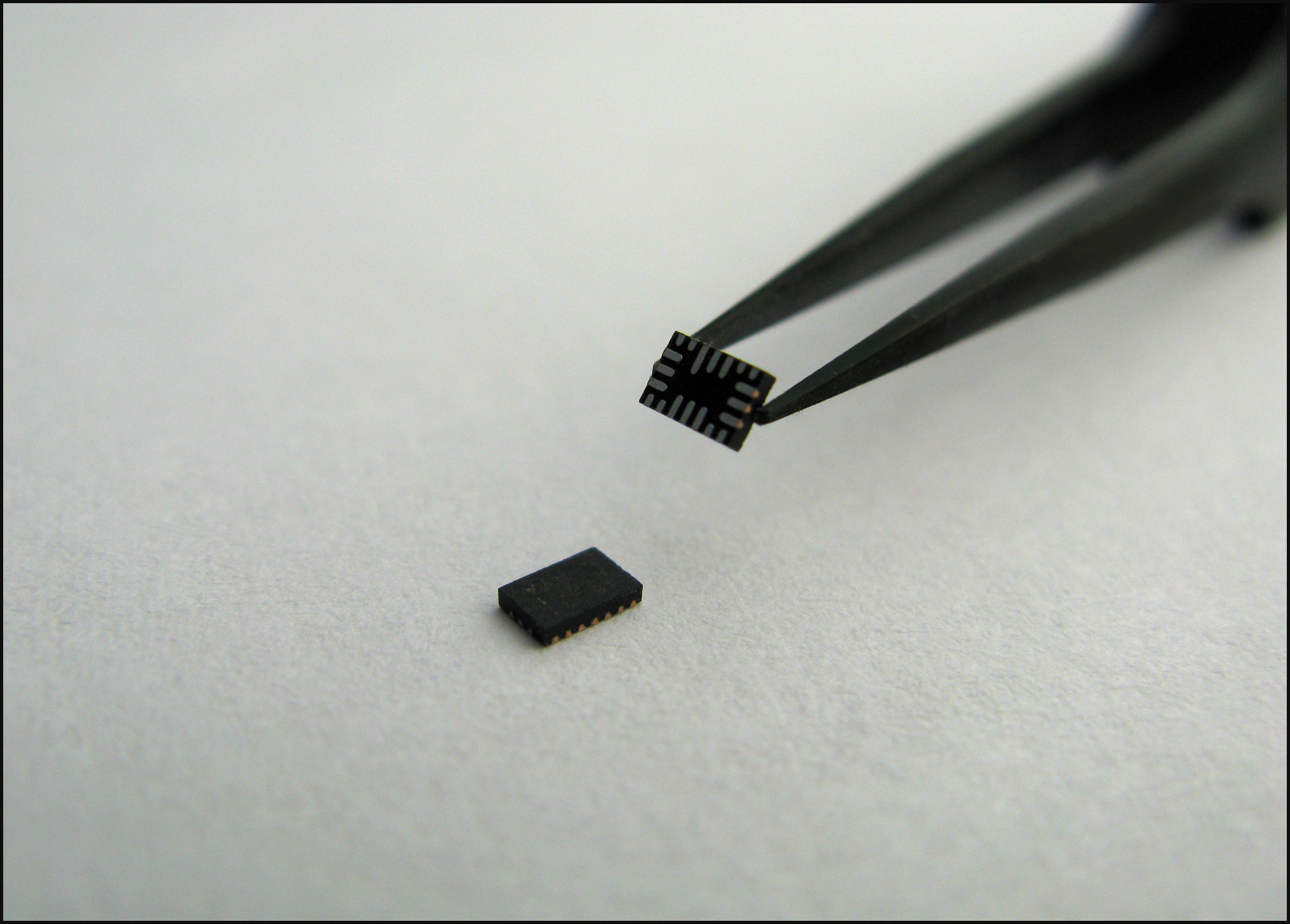
Computers used to take up entire rooms, then whole desktops, laps, and palms came along, and now to micro- chip sized casings and atom-powered transistors invisible to the naked eye. No is willing to be titled as a zero in terms of intelligence, but having a zero-sized intelligence in computing means packing a whole lot of brains in a tiny, tiny package. We’ll be watching with interest to see how it pans out.
# nanosizedevices # nanotechnology # nepalengineering # technology # zerosizeintelligence # zerosizephones # ZeroSizeTechnology